| * |
|
Overlay Instrument and Wafer Target Designs
Summary:A modern semiconductor chip has an enormous number of densely packed features that can measure smaller than 30 nanometers wide, built up in layers during as many as 27 lithographic process steps. Both the size of the features and the alignment of successive layers must be controlled to within a few nanometers. NIST custom-developed optical systems can measure such tolerances even though the light they use has wavelengths of hundreds of nanometers, and can make measurements fast enough to be part of fabrication lines that process thousands of chips per hour. NIST works closely with chip manufacturers to continually improve nanometrology tools and maintain U.S. technological leadership in the field. Description:The fabrication of semiconductor chips proceeds through a series of steps involving masks that are used to define patterns, along with photochemical processes that etch those patterns into the silicon wafers. The result is a layered structure incorporating a desired array of electronic components. Throughout this process, the tools holding the masks and the wafers must maintain a precise alignment that guarantees a tolerance of about 5 nanometers in the placement of chip features. As the number of components squeezed onto chips has increased, so has the technological difficulty of checking feature sizes and ensuring overlay alignment of successive masks with sufficient accuracy. Electron microscopy has been used, but it requires the chips to be held under high vacuum, and the electron beams can cause damage. Optical methods are more benign and easier to incorporate into a production line, but traditional imaging techniques cannot discern features smaller than the wavelength of the light, typically some hundreds of nanometers. A number of novel techniques pioneered by the Nanometrology Group make use of the fact that light reflected from a surface contains information about features and geometry smaller than the wavelength, even though that information does not show up in a conventional image. Alongside experimental development of this scatterfield technique has been major improvement in the theoretical understanding needed to infer the geometry of objects from the way they reflect light in the subwavelength regime. As a part of this project, several new target designs have been implemented including the new supertarget, recently joint patented with Sematech. In this design, the optical nature of multi0ple levels in close proximity are used to enable far field imaging of sub-resolution features leading to nanometer sensitivity. This project is developing a number of new target designs to take full advantage of recent advances in optical microscopy. Advances from the NIST program have steadily made their way into commercial chip manufacturing systems. The speed, accuracy, and relatively low cost of the new optical techniques open the door to innovations in chip design and manufacture that would not be possible with older methods for monitoring component size and placement. Additional Technical Details:Challenge/problem Addressed: A significant challenge for the semiconductor manufacturing industry is to develop advanced metrology techniques for overlay and registration to enable the continued long-term advance of device performance based on the stringent International Technology Roadmap for Semiconductors (ITRS) industry guidelines. Major Accomplishments:
|
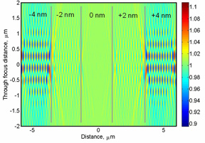
 TSOM image of a composite overlay target designed for double patterning showing sensitivity for different overlay values indicated. Start Date:February 1, 2008Lead Organizational Unit:pmlCustomers/Contributors/Collaborators:Customers:
Collaborators:
Staff:Dr. Richard M. Silver, Program Manager Contact
Physical Measurement Laboratory (PML) |
