*
Bookmark and Share

Theory of Transport in Graphene

Summary:

Graphene, a single layer of carbon atoms, is one of the most likely materials to produce the next breakthrough in the electronics industry.  Ideal graphene has the highest electron mobility of any known material, giving rise to high electron and thermal conductivities, which are both critical for making highly efficient electronic devices.  However, devices never achieve the ideal properties of graphene due to interactions between the graphene and the materials surrounding it, including the substrate and the contacts.  The different growth and fabrication techniques that have been tried lead to a wide variation in electronic properties due to interactions between the electrons and the environment around the graphene.  Our goal is to develop a theoretical description of the effect of the environment on the transport properties of graphene in order to enable the development of graphene into an important material for electronics applications.
 

Description:

When many carbon layers are stacked on top of each other, the result is graphite.  When just a two layers are stacked, the result is called “bilayer graphene” and when there are just a few layers, “few-layer graphene.”  Although monolayer graphene has been studied more than these other forms, the multilayer forms have advantages for applications.  Some of the growth techniques that are most likely to scale up to device production naturally produce few-layer graphene.  Additionally, by applying an electric field perpendicular to the layers, few-layer graphene can be modified to have a band gap, an important feature in all semiconductor electronic devices.  We calculate the transport properties of monolayer graphene, bilayer graphene, and few-layer graphene using a variety of approaches.  

As with semiconductors, it is easy to change the density of charge carriers in graphene.  This is important because many electronic properties, including conductivity, vary with charge density.  One important such property is screening – the ability of electrons to “cover up” defects.  In addition to trivial changes due to having more carriers, variations in carrier density cause changes in the screening properties that result in complex electronic interactions with the surrounding environment.  Due to screening, the ability to carry electrical current in these materials varies significantly as the density of electrons changes.  In addition, the variation in the screening properties depends strongly on the type of graphene.  We have shown how it may be possible to determine the type of graphene just from the way its conductivity changes as a function of the electron density.  The variation in screening properties also determines how the environment affects potential measurements in a scanning tunneling microscope.  Our calculations have shown that the differences in measurements between monolayer and bilayer graphene can be readily explained by this variation in screening properties between the two types of graphene.

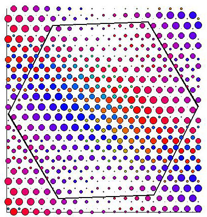
One of the first methods for fabricating graphene likely to be adopted by the electronics industry is to sublimate silicon from a silicon carbide crystal.  The carbon that is left behind forms few-layer graphene sheets that have many of the properties of single layer graphene.  Surprisingly, scanning tunneling microscopy measurements made in the CNST show that the electrons in the top layer behave as if they are in an isolated layer.  The top layer is rotated with respect to the layer below it, and our theoretical calculations explain why this leads to small coupling for all but the smallest rotation angles.  Using calculations of the electrostatic properties of the system, we have shown that this decoupling breaks down at the lowest temperatures and highest magnetic fields. 

Selected Publications
  • Mechanism for puddle formation in graphene, S. Adam, S. Jung, N. N. Klimov, N. B. Zhitenev, J. A. Stroscio, and M. D. Stiles, Physical Review B 84, 235421 (2011).
    NIST Publication Database        Journal Web Site
  • Semiclassical Boltzmann transport theory for graphene multilayers, H. Min, P. Jain, S. Adam, and M. D. Stiles, Physical Review B 83, 195117 (2011).
    NIST Publication Database          Journal Web Site
  • Landau levels and band bending in few-layer epitaxial graphene, H. Min, S. Adam, Y. J. Song, J. A. Stroscio, M. D. Stiles, and A. H. MacDonald, Physical Review B 83, 155430 (2011).
    NIST Publication Database          Journal Web Site

    More

Simulation showing the electronic coupling between individual atoms in the top and bottom layers of a twisted graphene bilayer
Electronic coupling between individual atoms in the top and bottom layers of a twisted graphene bilayer.

Lead Organizational Unit:

cnst

Customers/Contributors/Collaborators:

University of Texas, Austin
   Allan H. MacDonald

Staff:

Mark D. Stiles - NIST
Shaffique Adam - NIST (now at Yale NUS)
Hongki Min - NIST/UMD (now at Seoul National University)
Joseph Stroscio - NIST
Nikolai Zhitenev - NIST
Young Jae Song - NIST/UMD (now at Samsung)
Suyong Jung - NIST/UMD
Contact

Mark D. Stiles, Phone 301-975-3745

NIST
100 Bureau Dr., MS 6202
Gaithersburg, MD 20899-6202