| * |
|
Nanostructure Fabrication Processes
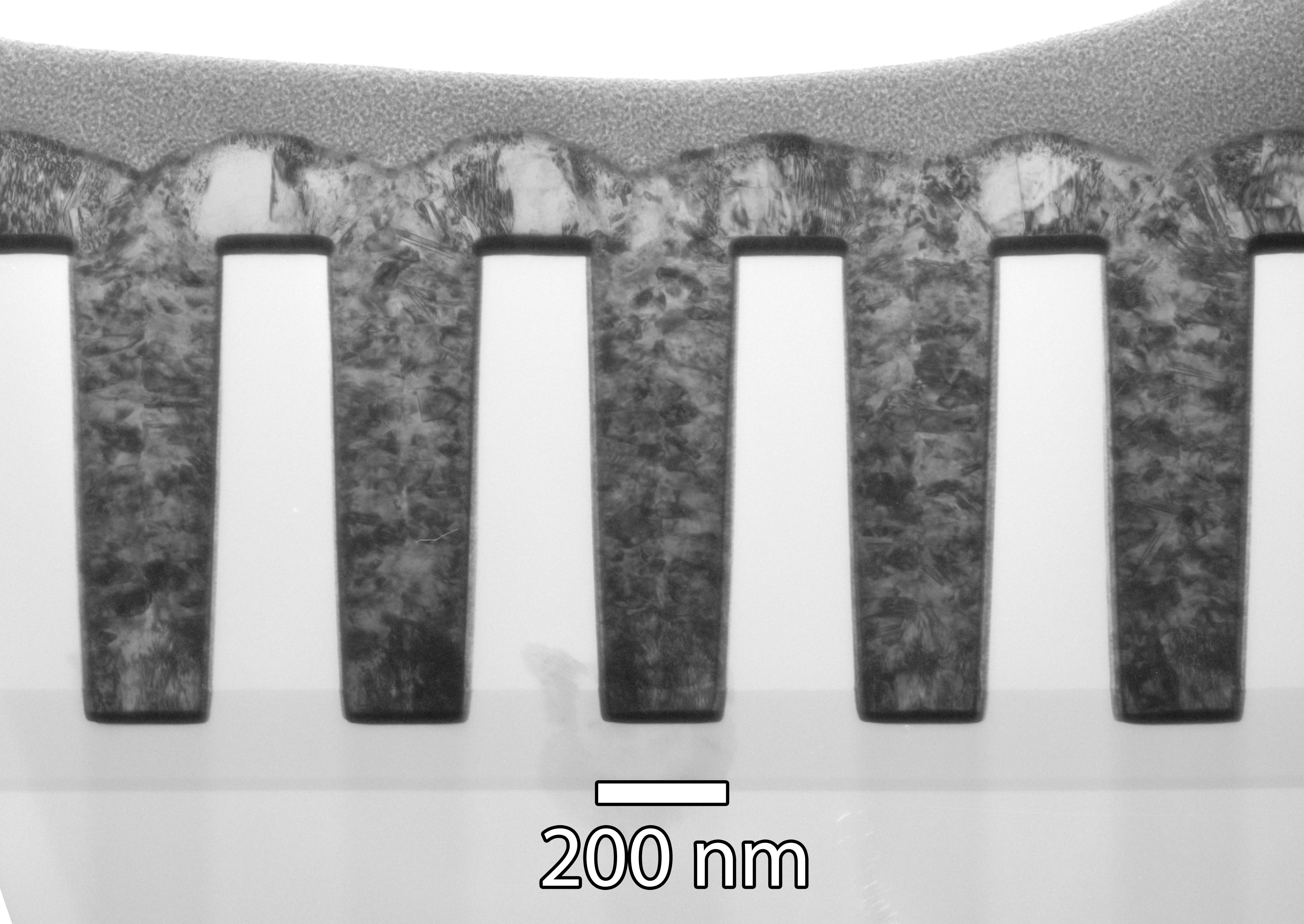
Summary:In this project we are developing in situ measurements relevant to the electrochemical fabrication, processing, and application of nanostructured materials and devices. Our effort is focused on the influence of adsorbates, defects, and stress state on the growth, structure, and morphology of complex nanostructures to enable control and optimization of the resulting material properties. Description:Progress in understanding and optimizing materials processing in wet chemical environments requires the use of in situ measurements of the structure and dynamics of the metal-electrolyte interface under realistic conditions. These measurements can provide insight into the mechanisms of relevant atomic, molecular, and mesoscale film growth and dissolution processes. This project has several thrust areas ranging from measurements and modeling of surfactant mediated growth to the investigation of both surface and thin film growth stress. Particular attention has been given to the role of electrolyte additives in the formation and performance of advanced nanoscale and mesoscale interconnects as used in state of the art microelectronic devices. Measurements are also underway that detail the use of underpotential deposition (upd) reactions to precisely control the composition and structure of 2-D and 3-D alloys. This is complemented by measurements of stress changes that accompany alloy formation as well as the inverse dealloying process. An integral part of the program is the development of mechanistic linkage between atomic and molecular phenomena and rational design of the desired nanostructures. Additional Technical Details:This year we demonstrated the first example of void-free trench filling with ferromagnetic materials. Feature filling involves a new mechanism of superconformal growth that uses a single inhibitor whose consumption during deposition gives rise to positive feedback. Coupling of the non-linear dynamics with the non-planar substrate geometry gives rise to void-free nickel deposition in the recessed surface features as shown in the cross section TEM images given below. Two types of molecules have been shown to yield this effect; cationic Nbearing polymers and more recently certain benzimidazole derivatives. The latter provide feature filling dynamics that offer seamless integration with conventional Damascene processing and thereby the prospect of introducing ferromagnetic materials into 3-D metallization for ULSICMOS and MEMS applications.
The upd process has also been applied to Pt-Ni and Pt-Co alloys and preliminary studies indicate that these alloy films are more catalytic than pure Pt for the oxygen reduction reaction; the latter being a central impediment to improved fuel cell performance.
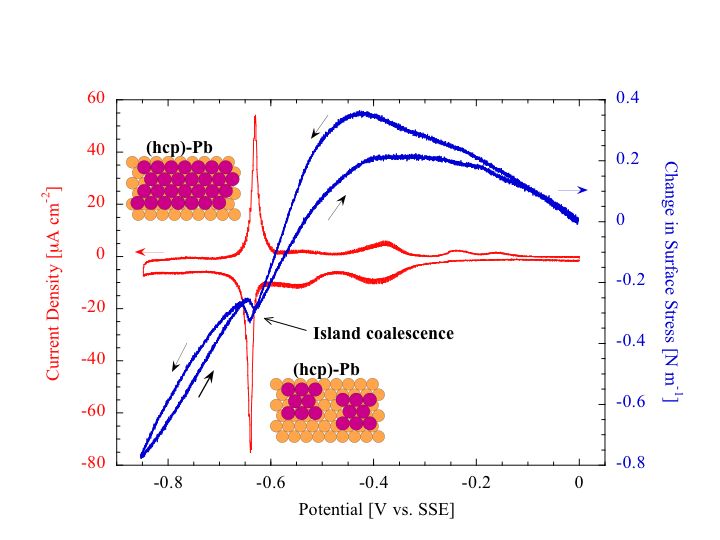
MML has recently constructed an optical bench for in situ measurement of surface stress during electrochemical processing using the wafer curvature method. Forces on the order of 0.008 N/m (23 km radius of curvature) can be resolved, sufficient to study the adsorption of upd and molecular monolayers. This powerful method is capable of monitoring the surface stress associated with reversible upd reactions such as Pb onto the (111)-textured Au surface as shown below. The stress transient shows four regimes of behavior from ClO4- desorption, Pb-Au bond formation, stress relaxation due to hcp-Pb island coalescence, and electrocompression of the monolayer at potentials just positive of bulk Pb deposition. Interestingly, these measurements show that the complete Pb monolayer behaves as a free-standing elastic film where the stress - strain proportionality has a value equal to the biaxial modulus for Pb (111) in the bulk. Similar work has examined the upd of Bi on Au. Further work is underway exploring these timely and exciting issues.
Major Accomplishments:
|
 End Date:ongoingLead Organizational Unit:mmlStaff:Thomas P. Moffat Gery Stafford Daniel Josell Daniel Wheeler Chang Hwa Lee Ugo Bertocci John Bonevich Associated Products:Project Summary (PDF) Contact
For more information, contact: Thomas P. Moffat T: 301-975-2143 F: 301-975-926-7679 |