| * |
|
Wafer Level AFM Metrology for Critical Dimension Measurements
Summary:Significant manufacturing metrology challenges exist beyond scale calibration for the accurate determination of the size width and length of physical features. Measurement of linewidth or critical dimension (CD) continues to be one of the most fundamental dimensional metrology needs in the semiconductor and nanomanufacturing industries. Semiconductor manufacturers refer to this continually decreasing measurement limit as critical dimension (CD) metrology. The critical dimension size and tolerance decreases as technology progresses. The AFM is considered an essential tool in the measurement of nanometer scale features for the determination of feature shape. The AFM has also developed into an important element in reference metrology. Description:A reference measurement system based upon the CD-AFM presently within the program offers the most straightforward and highest resolution traceability path for the physical linewidth determination. Reference measurement systems (RMS) based on CD-AFMs have been established (by NIST staff) at both NIST and SEMATECH. These instruments will be the major source of reference metrology at NIST and at SEMATECH. Both of these tools were calibrated using NIST methodologies, standards, and measurements on other NIST instruments. Scanned probe tip widths with standard uncertainties less than 1 nm are measured through reference to the NIST-developed single crystal critical dimension reference material (SCCDRM). As part of this process a rigorously traceable atomic-lattice-based calibration technique for linewidth using high angle annular dark field scanning transmission electron microscope was developed. A new calibration technique for nanoscale feature sidewall angle was also developed. An important part of AFM metrology is tip characterization. NIST will be expanding modeling techniques developed in the 1990’s for reconstruction of tip shape from calibration images to include an entire array of new sample geometries in response to rapidly evolving industrial requirements that are now less the 1 nm standard uncertainty for sub 50 nm sized features. NIST will also develop accurate measurement protocols and an uncertainty statement for prototype polysilicon linewidth standards, and perform new linewidth measurements of SRM 2059 and the chrome on quartz photomask that will be used for the BIPM intercomparison. We will also serve as the pilot laboratory for a preliminary key comparison of the nanoscale linewidth measurement capabilities of national measurement institutes around the world, sponsored by the Bureau International des Poids et Mesures (BIPM) in Paris.
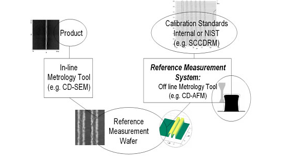
Based on a critical dimension atomic force microscope (CD-AFM) the reference measurement system is used to impart traceability to dimensional measurements made in semiconductor manufacturing facilities. The types of measurements include step height, pitch, and linewidth. For linewidth, the same features measured with the RMS are measured using work-horse instruments such as the scanning electron microscope, thus enabling cross-calibration of those tools Additional Technical Details:Challenge/problem Addressed: To address traceability problems in semiconductor dimensional metrology, NIST in collaboration with SEMATECH developed and implemented a critical-dimension atomic force microscope (CD-AFM) based reference measurement system (RMS). The key goal of the system is to transfer traceable length measurements to tools used in the semiconductor industry. Major Accomplishments:
|
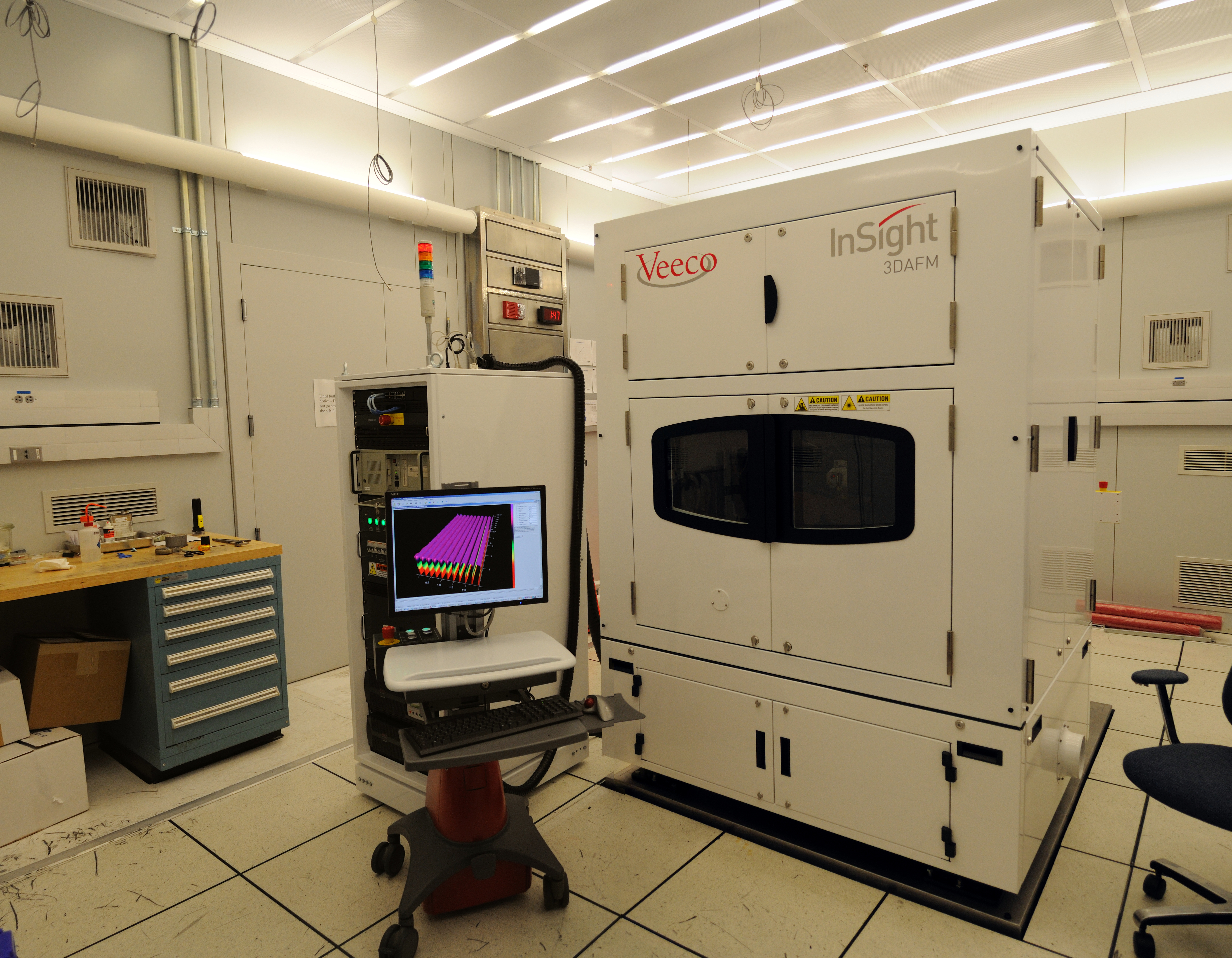
 Veeco Insight 3D Atomic Force Microscope is used for linewidth metrology in the semiconductor industry and is used at NIST to support the single crystal critical dimension reference material (SCCDRM) project. Start Date:February 1, 2008Lead Organizational Unit:pmlCustomers/Contributors/Collaborators:Customers:
Collaborators:
Facilities/Tools Used:Critical dimension atomic force microscope Contact
Physical Measurement Laboratory (PML) |

