Electron Microscopy Lab
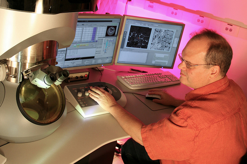
Rob Dickerson examines a multiphase oxide scale using the FEI Titan 80-300 transmission electron microscope.
Contact
- Rob Dickerson
- (505) 667-6337
- Rod McCabe
- (505) 606-1649
- Pat Dickerson
- (505) 665-3036
- Tom Wynn
- (505) 665-6861
Go to full website »
Capabilities, facilities, research opportunities
The Electron Microscopy Lab (EML) is a user facility maintained by the Lab's Metallurgy Group (MST-6) of the Materials Science Division. It is located in the Material Science Laboratory (TA-03, Building 1698, Room C135). The Electron Microscopy Lab's focus is the study of microstructures with electron and ion beam instruments, including crystallographic and chemical techniques.
The EML staff maintain and operate the instruments within the facility for the use of the EML staff and a user group, which includes other Los Alamos National Laboratory staff members, postdoctoral associates, technicians, graduate students, and visiting researchers. The EML staff also provide advice on appropriate sample preparation and instrument selection for given research needs and training and supervision on the various instruments. The EML staff may also be contracted to conduct research for others.
The EML has three transmission electron microscopes (TEMs), two scanning electron microscopes (SEMs), and one focused ion beam/scanning electron microscope (FIB/SEM):
- JEOL 3000F TEM - dedicated to high and atomic resolution imaging
- FEI Tecnai F30 - analytical TEM with scanning capabilities, with energy dispersive spectrometry (EDS) and electron energy loss (EELS) imaging and analysis. Also used for in-situ tensile testing and pico-indentation
- FEI Titan 80-300 - monochromated, image aberration-corrected imaging, and analytical TEM with full EDS and EELS imaging and analysis, including sub-Å TEM, 1.4 Å STEM, TEM and STEM tomography, and Lorentz imaging
- FEI XL30 SEM - equipped with an electron backscatter detector (EBSD) for crystallography and texture measurements
- FEI Inspect F SEM - outfitted with EDS, EBSD, and a Gatan XuM x-ray tomography system
- FEI Helios 600 FIB/SEM - used for preparation of TEM and micromechanical test specimens; also features EDS and ESBD detectors and software for 2D and 3D chemical and crystallographic imaging
In addition, specimen preparation equipment and optical microscopes are available for use.
More Like This

Video

Tree Death Study's Climate Change Connections
What are the exact physiological mechanisms that lead to tree death during prolonged drought and rising temperatures? These are the question...