*
Bookmark and Share

CMOS Device and Reliability

Summary:

The CMOS Device and Reliability Project will develop advanced metrology tools to enable high performance CMOS devices with sufficient reliability.

CMOS (Complementary Metal Oxide Semiconductor) technology is part of the basic competency of our industrial country. CMOS devices are the fundamental building blocks of nearly every electronic system found in modern society. The continued development of CMOS enables or improves almost all advanced technologies. While CMOS technology advances at a rapid pace, it is extremely complex. This project develops methods to characterize new CMOS devices and ensure their reliability for a wide range of applications. In doing this, we are able to help U.S. companies compete successfully in this vital industry.

Description:

Electron devices and their reliability have long been important topics of research at NIST. Over the years, we have always played a central role in this important field. Many of the commonly used test structures and test methodologies in the industry were developed at NIST. NIST also led many of the standard setting efforts.
CMOS technology has advanced at a steady, but rapid pace for many decades. It is now a global business with over $270 billion in annual sales. The larger electronics industry that leverages the CMOS technology has annual sales of multi-trillion dollars. Everything electronics, as we all have come to expect, get cheaper and better every year - a benefit of the relentless advance in CMOS technology.

The CMOS transistors currently in production are as small as 30 nm, and those in advanced development are smaller than 10 nm. Properly characterizing these devices and understanding factors that affect their performance and reliability are extremely challenging. Our work focus is on meeting these measurement challenges by pushing the known measurement technologies to the limit and developing new measurement capabilities. By emphasizing fundamental understanding of the measured phenomenon, we amplify our impact to the industry.

Major Accomplishments:

  • Developed the world’s fastest pulsed current-voltage sweep measurement. Achieving a complete, high-fidelity sweep of the transistor in 2 μs.
  • Developed a high-accuracy measure-stress-measure method for characterizing the bias-temperature-instability phenomenon in MOSFETs (metal-oxide semiconductor field-effect transistors).
  • Discovered a hidden electron-trapping and –detrapping mechanism in the negative-bias-temperature-instability of p-MOSFETs.
  • Demonstrated that the model that has been used for over five decades by everyone to explain random telegraph noise and low-frequency noise is completely wrong.
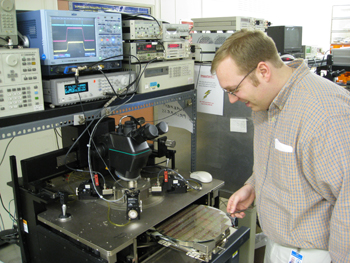
Jason Campbell of the CMOS Project.
Loading 12” wafer containing state-of-the-art CMOS devices into a probe station in preparation of making high-speed measurements of transient changes in device characteristics due to temperature-bias stress.

End Date:

on-going

Lead Organizational Unit:

pml

Staff:

Kin (Charles) P. Cheung, Leader
Jason Campbell
Joseph Kopanski
Nhan V. Nguyen
Jason Ryan
John S. Suehle

Contact

Charles Cheung
301-975-3093 Telephone

100 Bureau Drive, M/S 8120
Gaithersburg, MD  20899-8120