| * |
|
Thin Film Electronics
Summary:The Thin Film Electronics Project enables the commercialization of emerging and future semiconductor electronic device technologies, such as flexible/printed electronics, replacements to scaled Si logic and memory, and Gen II and III solar cells by tailoring existing measurements, establishing new measurements, and designing and building device analogous high quality test structures to provide the measurement science infrastructure necessary for underpinning innovation in industry, academia, and government laboratories. Description:
The Thin Film Electronics Project conducts basic research to develop and advance novel measurements that combine and correlate optical and electrical methods such as internal photoemission, spectroscopic ellipsometry, temperature dependent current-voltage spectroscopy, impedance spectroscopy, and transient photo-current/voltage spectroscopy. Particular emphasis is placed on direct, non-destructive optical-electrical and electrical measurement methods to quantify band structure, charge transport, and density of in-gap electrically active traps for the rational design and advanced manufacturing of emerging and future semiconductor electronics devices.
Candidate technologies presently investigated include: Homo/heterojunction tunnel FETs, high mobility CMOS, heterojunction solar cells, printable electronic materials and devices such as organic TFTs and solar cells, transparent metal oxide TFTs, and graphene and other layered 2D electronic materials for thin film flexible electronics.
Major Accomplishments:
Selected Publications
|
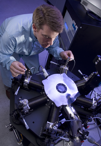
 Characterizing the electronic properties of single crystal organic field-effect transistors in a vacuum cryogenic probe station (Copyright Robert Rathe) Start Date:January 1, 2005End Date:ongoingLead Organizational Unit:pmlStaff:David J. Gundlach, Leader Contact
David Gundlach 100 Bureau Drive, M/S 8120 |


