 - Electronics & Telecommunications
 Find out what NIST is currently working on in Electronics & Telecommunications.
Jack Pevenstein
Technology Partnership Office
301-975-5519
nisttech@nist.gov
100 Bureau Drive, M/S 2200
Gaithersburg, MD, 20899
A highly compact, portable, pulsed-molecular-beam Fabry-Perot cavity Fourier transform microwave spectrometer which incorporates ultra-fine Fabry-Perot mirror surface finishes has been developed for trace gas analysis. The mirrors, having a surface finish of less than or equal to 0.25 microns rms, are coated with nickel and then with either gold or silver. In a further embodiment, one or more fixed-tuned Fabry-Perot cavities are incorporated within a single vacuum chamber to monitor one or more chemical species of interest.
A workflow sequence specified by a process definition is managed by a workflow management system which enacts each segment in the order specified by that process definition. Role-based access control (RBAC) is used to define membership of individuals in groups, i.e., to assign individuals to roles, and to then activate the roles with respect to the process at appropriate points in the sequence. Any individual belonging to the active role can perform the next step in the business process. Changes in the duties and responsibilities of individuals as they change job assignments are greatly simplified, as their role memberships are simply reassigned; the workflow process is unaffected.
A system and method for time-stamping and signing a digital document by an authenticating party and returning the signed stamped document to the originator or his designated recipient. Messages may be received by a first "public" machine over a network, by fax, or through input mediums such as diskettes. The clock of the first machine is synchronized with Universal Coordinated Time (UTC) and can be checked for accuracy by anyone on the network. A second "private" machine, not connected to any network, receives the time-stamped message, applies a hashing procedure and provides a signature using a private key. The signed hashed time-stamped message is then returned. A verify procedure is made widely available to check the genuineness of a document by rehashing the document and applying a public key. The result should match the signed time-stamped message returned by the authenticating party.
The method of the invention identifies damage to an in-service conductor associated with the delivery (transmission and distribution) of electric power. Electro-magnetic acoustic energy is generated in an in-service conductor associated with the delivery of electric power. Corresponding return electro-magnetic acoustic energy is then measured. Features are then extracted from the return electro-magnetic acoustic energy to characterize damage to the in-service conductor. The features may be extracted through a variety of signal processing techniques, such as wavelet signal processing. The extracted features may be classified using a neural network, fuzzy logic, or a combination of both.
A new low temperature method for nanostructured metal and ceramic thin film growth by chemical vapor deposition (CVD) involves the use of a low pressure co-flow diffusion flame reactor to react alkali metal vapor and metal halide vapor to deposit metal, alloy and ceramic films. The reaction chemistry is described by the following general equation: (mn)Na+nMXm .fwdarw.(M)n +(nm)NaX where Na is sodium, or another alkali metal (e.g., K, Rb, Cs), and MXm is a metal-halide (M is a metal or other element such as Si, B or C; X is a halogen atom, e.g., chlorine, fluorine or the like; and m and n are integers). This reaction chemistry is a viable technique for thin film growth. In one mode, using the precursors of sodium metal vapor, titanium tetrachloride (the limiting reagent), and either argon or nitrogen gases, titanium (Ti), titanium nitride (TiN), titanium dioxide (TiO2), and titanium silicide (TiSi, Ti5 Si3, TiSi2, Ti5 Si4) thin films have been successfully grown on copper and silicon substrates. Conditions can be adjusted to prevent or minimize gas-phase particle nucleation and growth. Substrate temperatures can also be varied to prevent excessive salt deposition.
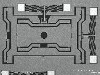
Multilayer, thin film multijunction integrated micropotentiometers are formed in an integral multifilm membrane form over a through opening in a nonmagnetic, dielectric substrate. Through the use of conventional photolithographic and etching techniques, integrated structures are formed to include either single elongate heater elements, bifilar heater elements, or trifilar heater elements with multiple return paths. Multijunction thermopiles and resistors are formed with the heater. The individual layers of silicon oxide or silicon nitride, are formed with conventional chemical vapor deposition, sputtering and other known techniques.
A method and apparatus for accurately generating a digitally synthesized sinusoidal voltage is started by storing digital values for sine waveforms in a read only memory. A first and second digital to analog converters are connected to the read only memory through latches. The outputs of the first and second digital to analog converters are alternatively switched between the inverting input and the non-inverting input of an operational amplifier such that one of the first and second digital to analog converter is connected to the inverting input while the other is connected to the non-inverting input. The output of the operational amplifier is connected to the inverting input through a variable capacitance, the feedback being determined by the one of the first and second digital to analog converter connected to the inverting input. A clock is used to control the connection of the first and second digital to analog converter to the inverting input and to control the determination of the feedback.
A manufacturing method for convective accelerometers and tilt sensor devices using CMOS techniques. An integrated circuit chip is produced which includes a silicon substrate having an integrated circuit pattern thereon including a heater element located centrally of the substrate and at least first and second thermocouple elements located on the substrate on opposite sides of the heater element. Thereafter, portions of the substrate surrounding and beneath the heater and thermocouple elements are etched away to suspend the element on the substrate and thus to thermally isolate the elements from the substrate. The substrate is etched up to the cold thermocouple junction of the thermocouple elements so the cold junction remains on the substrate.
A Josephson quantizer is driven by a sinusoidal microwave generator whose output is combined with a digital two-level code representing a desired waveform. The result is to produce a bipolar drive signal of increased frequency and a bipolar Josephson output with voltage increased significantly. Output voltage is developed according to the relationship V=Nnmfs /KJ, where N is the number of junctions, n is the Josephson junction constant voltage step number, fs is the sampling frequency, m is an integer multiple of the sampling frequency and is .gtoreq.2, and KJ is the Josephson constant. The digital code generator receives the output of an improved modulator which incorporates a three-level to two-level transformation on the output of a standard three-level modulator in one embodiment. In a second embodiment, a modified two-level modulator produces a bit sequence where the polarity of the next bit is allowed to change only if there is an odd number of consecutive bits of the same polarity.
The operation of a planar geometry superconducting coil used in conjunction with a ground plane is improved by intracoil damping. This damping reduces coil resonances. The improvement consists of an intracoil shunt, which damps the resonances of the coil by connecting each turn, or loop, of the multiturn/multiloop coil with resistors. One example of a planar geometry superconducting coil which is effectively damped according to the present invention is the input coil to a superconducting quantum interference device (SQUID). The intracoil shunt may be added to the SQUID at the same time in the SQUID fabrication as the junction shunts.
A method for forming a single cavity in a substrate, which may extend approximately the length of a device located on top of the substrate, and device produced thereby. The device has a length and a width, and may extend approximately the length of the substrate. After locating the device on the surface of the substrate, a first etchant is applied through openings on the surface of the substrate. Subsequently, a second etchant is applied through the same openings on the surface of the substrate. As a result, a single cavity is formed beneath the surface of the device, suspending the device and minimizing electrical coupling.
Spectroscopic materials analysis wherein a sample under test is bombarded by electrons in a scanning electron microscope to produce an x-ray emission collected over a large solid angle by a polycapillary lens and focused onto the surface of a microcalorimeter detector. The x-ray lens is used to increase the effective collection area of the microcalorimeter detector used in an x-ray spectrometer. By increasing the collection angle, the time period for x-ray collection is reduced and the detector can be located farther from the x-ray source. The x-ray lens is effective over a broad energy range of x-rays, thus providing compatibility with spectroscopic analysis. The microcalorimeter can be calibrated to compensate for any variations in the transmission efficiency of the x-ray lens.
A low noise accurate signal generator for a calibration system or a radar system includes a generator of a digital data stream having a predetermined frequency spectrum incorporated therein. A series connected array of Josephson junctions is coupled to and excited by the digital data stream to provide a stream of pulses with quantum mechanically accurate time integral. A low pass analog signal filter is coupled to the pulses of accurate time integral for extracting analog signals of the predetermined frequency spectrum. For radar applications, a low phase-noise local oscillator of a fixed RF frequency and the output of the filter are coupled to a signal mixer which outputs low phase-noise chirped RF signals for use in generating transmit pulses for the radar system whereby enhanced detection of targets in "clutter" can be obtained.
A detector of X-ray and the like in which very good resolution of energy can be obtained. The device is based on two basic components. The first is the x-ray absorber in which an x-ray interacts with a film and converts its energy into heat. Because the absorber is operated at cryogenic temperatures, approximately the range of 0.01 Kelvin to 1 Kelvin, its heat capacity is small and causes a measurable temperature rise. The second component of the invention is a base layer of normal metal which absorbs the heat generated by the x-ray. The third component of the invention is the method to detect the temperature rise. This thermometer is based on a normal metal-insulator-superconductor tunnel junction, where part of the base layer is the normal metal. When the tunnel junction is electrically biased at a voltage slightly below the gap voltage of the superconductor, the electrical current that flows through the junction is sensitively dependent on the temperature of the normal metal.
A device and method provide for an accurate output from a unit, such as an oscillator and/or clock providing an output indicative of frequency and/or time. The device includes a processing section having a microprocessor that develops a model characterizing the performance of the device, including establishing predicted accuracy variations, and the model is then used to correct the unit output. An external reference is used to provide a reference input for updating the model, including updating of predicted variations of the unit, by comparison of the reference input with the unit output. The ability of the model to accurately predict the performance of the unit improves as additional updates are carried out, and this allows the interval between the updates to be lengthened and/or the overall accuracy of the device to be improved. The accuracy of the output is thus adaptively optimized in the presence of systematic and random variations.
A low-loss comb-generating optical cavity including an optical amplifier and a microwave-driven electro-optic modulator crystal, produces a comb of optical frequency sidebands having spectral lines equally spaced around the frequency of an input laser beam incident on the comb-generating cavity. The comb-generating cavity includes an input mirror movable along the beam propagation direction, and a fixed position output mirror located at time synchronous distances of both the input laser wavelength and modulation wavelength. The comb-generating cavity and its microwave driven modulator are in resonance with the input laser beam, and provide iterative or recirculating beam action that transfers the input optical frequency of the laser, sideband by sideband, to remote and precisely known comb frequencies offset from, and centered on, the input laser frequency. Optical parametric amplification within the comb-generating cavity extends the sideband or comb spectrum and sharpens the time domain impulse represented by the cavity circulating fields. A relatively short bandpass filter optical cavity receives the comb output of the comb-generating cavity and is made up of the fixed-position mirror and a third mirror movable along the beam propagation direction. Fine movement of the third mirror tunes the bandpass filter cavity, and preferentially couples out the power of one or more comb frequencies. An optional input optical cavity at the input side may increase efficiency. A self-oscillating configuration provides optical parametric oscillation.
The present invention is directed to a metal hydrides lamp and a fill for such a lamp. The lamp chamber includes a fill of at least one metal, a buffer gas, and hydrogen and/or deuterium. When energy is provided to the fill, metal combines with the hydrogen and/or deuterium to form a molecule at an excited energy level which emits visible light when the molecule moves to a ground state energy level. The lamp may be an electrode lamp, an electrodeless lamp, a microwave lamp, or any other power source capable of imparting energy into a fill contained within a lamp chamber.
A chemical process for producing bulk quantities of an iron-silica gel composite in which particle size, form, and magnetic state of the iron can be selected. The process involves polymerizing an ethanolic solution of tetraethylorthosilicate, ferric nitrate and water at low temperature under the influence of an HF catalyst. The chemical and magnetic states of the iron in the resultant composite are modified in situ by exposure to suitable oxidizing or reducing agents at temperatures under 400° C. Iron-containing particles of less than 200 angstrom diameter, homogeneously dispersed in silica matrices may be prepared in paramagnetic, superparamagnetic, ferrimagnetic and ferromagnetic states.
A high lead solder exhibiting improved wettability to metal substrates, an advantageously controlled melting range, and excellent thermal fatigue properties. It comprises about 98-100% lead and a minor amount, typically about 0.0005-0.1 wt %, based on the total weight of the solder composition, of an alkali metal selected from the group consisting of Na, K, and Li. Additional embodiments additionally comprise an amount of a grain-size controlling additive, e.g., 0.001-0.5 wt % (based on the total weight of all the components in the solder composition) selected from the group consisting of Ce, Ba, La, Pr, Nd, Sm, Eu, Gd, Th, Dy, Ho, Er, Tm, Yb, Y, Lu, Sc, Mg, Na, Se, Te, oxides thereof and mixtures thereof, in amount effective to control the Pb grain size; and 0-1 wt % of an element selected from the group consisting of Sn, In, Bi, Sb, Ag, Au, and Ga, and mixtures thereof.
This invention provides a mechanical support for a two-pill Adiabatic Demagnetization Refrigerator (ADR). The support utilizes a suspension of the two pills from one side of the magnet bore only. In the two pill ADR, the thermal ground is at 4K, a guard pill positioned in the front of the bore cools to 1K and a base pill positioned in the back of the bore cools to 50-100 mk. A connector rod of the base pill traverses the guard pill, and connector rods to both the guard pill and base pill exit through the front aperture. A preferred embodiment of the two-pill support for the front loaded magnet bore utilizes planar support modules comprising three members connected by Kevlar strings. Each member is thermally connected either to one of the pills or to thermal ground. The ground member, the guard member and the base member of the support module are strung with Kevlar threads, such that the base member is suspended only from the guard member, and the guard member only from the ground member. These planar support modules can be aligned and assembled prior to use in an assembly jig. The final assembly of the two-pill support structure using planar support modules is easy and fast.
A high-Tc superconductor contact unit having low interface resistivity is disclosed, as is a method for making the unit. An inert metal is deposited on the surface of the superconductor, which surface is preferably non-degraded, to form a unit with the surface of the superconductor, and where temperatures as high as 500°C to 700°C can be tolerated, the unit is oxygen annealed to establish a still lower surface resistivity between the surface of the high-Tc superconductor and the inert metal, including a low surface resistivity of about 10-10 Ω-cm2 at high-Tc superconductor operating temperatures. The superconductor is a metal-oxide superconductor, and may be rare earth, thallium, or bismuth based.
A positioning device and method for positioning objects is provided. The device includes a movable stage and a pair of levers. The pair of levers is symmetric about a first axis of the movable stage. Additionally, the pair of levers is parallel to a second axis of the movable stage. This second axis is perpendicular to the first axis. Each of the pair of levers applies a force to the movable stage. Each of the pair of levers moves in an arc. The two levers move in opposite directions along their respective arc. The two arcs are symmetrical about an axis of the movable stage.
A position detector for sensing the position of a movable member which moves along an axis relative to a stationary member. A nonrepeating N bit chain code embodied in a scale on the movable member runs along the axis. A detector fixed to the stationary member is positioned to sense a portion of the chain code. The detector has K elements (K>>N) generating a plurality of signals. A controller determines the position of the movable member relative to the stationary member as a function of the signals.
A spatial RAM system uses the position of a data sensor to generate a clock pulse that is used to trigger data acquisition. As a consequence, the errors associated with time-based clock sampling are avoided. This enables more accurate sampling of data at locations desired in space and more easily allows for non-uniform sampling.
A spatial RAM system uses the position of a data sensor to generate a clock pulse that is used to trigger data acquisition. As a consequence, the errors associated with time-based clock sampling are avoided. This enables more accurate sampling of data at locations desired in space and more easily allows for non-uniform sampling.
The invention relates to a three-dimensional measuring device, comprising a rotating 360 degree sensor head, a laser scanner and an extendable mast system. The sensor head contains a 360 degree rotating multi-faceted mirror, which determines total path distance from the laser scanner to a particular target. Angular orientations on both the scanner and the faceted mirrors are calculated by a precision encoding system. The measured total path distance, mast system extension, scanner head rotation, mirror rotation angles, and mast deflection are all used to calculate the location of a target point in 3-D space relative to the scanner. The sensing device can be utilized in the construction and nuclear power areas. In the nuclear power area, the mast system can be extended into a contaminated area which the sensor remains outside the contaminated area, thereby avoiding contamination problems.

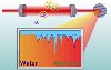
A system for heating water using solar energy comprises a photovoltaic array, a water heater comprising a variable resistive load, and a controller for varying either the load characteristics of the resistive load or the power generating characteristics of the photovoltaic array, or both, to ensure maximum power transfer efficiency.
Multi-layer transition-edge sensors (TES) having improved performance, a method for preparing them and methods of using them. Specifically, the improvement lies in providing normal metal strips along the edges of the superconducting and normal metal layers parallel to the current flow in the TES during operation. These strips (referred to as "banks") provide for both improved detector performance and improved detector robustness against corrosion. This improvement is an important advance particularly for TES-based microcalorimeter detectors. The improved TESs also have many other applications based on the very precise thermometer function achieved by the TES.

A positioning device and method for positioning objects is provided. The device includes a movable stage and a pair of levers. The pair of levers is symmetric about a first axis of the movable stage. Additionally, the pair of levers is parallel to a second axis of the movable stage. This second axis is perpendicular to the first axis. Each of the pair of levers applies a force to the movable stage. Each of the pair of levers moves in an arc. The two levers move in opposite directions along their respective arc. The two arcs are symmetrical about an axis of the movable stage.
A system and method for using one or more localized weak-link structures, and damping on the electrical bias circuit, to improve the performance of superconducting transition-edge sensors (TES). The weak links generally consist of an area or areas having a reduction in cross-sectional geometry in an otherwise uniform bilayer TES applied to a substrate. The weak links control the dissipation of power in the sensor, making it quieter and making its electrical response smoother and less hysteretic. The TES response is also made smoother by implementing a damping circuit on the electrical output of the TES.
The present invention provides a novel humidity chamber suitable for use with an atomic force microscope (AFM). The humidity chamber of the present invention employs an intricate geometrical design which can accommodate a scanned-stylus AFM with an optical lever. This geometrical design allows the invention to enclose one or more of the AFM scanner, tip assembly, optical lever detection system, sample and an optical microscope objective lens, without degrading the ability to operate the AFM or the related systems. The invention is comprised of two major pieces: a chamber within which the AFM scanning head assembly is placed, and an integrated sample platform and spring-loaded base-plate that allows samples to be loaded and unloaded without removal of the chamber from the AFM scanning head assembly. The sample platform, which extends up from the base-plate and is inserted into the chamber, can include a magnet that is securely attached to the base. Once the sample platform is positioned inside the chamber, a locking pin can be inserted between the chamber and the bottom portion of the sample platform to secure the sample platform and base-plate. The spring-loaded base allows the z-directional motors of the AFM to be used to position the sample just below the probe prior to scanning, while at the same time providing an essentially air-tight fit between the chamber and the AFM scanning head. An embodiment of the present invention is suitable for use with components that sense and control the relative humidity inside the chamber.
The present invention provides a novel humidity chamber suitable for use with an atomic force microscope (AFM). The humidity chamber of the present invention employs an intricate geometrical design which can accommodate a scanned-stylus AFM with an optical lever. This geometrical design allows the invention to enclose one or more of the AFM scanner, tip assembly, optical lever detection system, sample and an optical microscope objective lens, without degrading the ability to operate the AFM or the related systems. The invention is comprised of two major pieces: a chamber within which the AFM scanning head assembly is placed, and an integrated sample platform and spring-loaded base-plate that allows samples to be loaded and unloaded without removal of the chamber from the AFM scanning head assembly. The sample platform, which extends up from the base-plate and is inserted into the chamber, can include a magnet that is securely attached to the base. Once the sample platform is positioned inside the chamber, a locking pin can be inserted between the chamber and the bottom portion of the sample platform to secure the sample platform and base-plate. The spring-loaded base allows the z-directional motors of the AFM to be used to position the sample just below the probe prior to scanning, while at the same time providing an essentially air-tight fit between the chamber and the AFM scanning head. An embodiment of the present invention is suitable for use with components that sense and control the relative humidity inside the chamber.
A non-destructive method enables the detection of moist areas located inside a building wall or the like. A transmitter generates a series of ultra-wideband pulses that are sent to an antenna unit, preferably in the form of an array that includes a plurality of switchable antenna pairs. The antenna unit directs the pulses toward the building structure and receives pulses that are reflected from the structure. Computational algorithms process the reflected pulses received by the antenna unit and produce an output, typically in the form of visual map that can be used to identify the locations of excessive moisture in the wall or structure.
Apparatus and method for integrating lasers and optics on glass substrates. An optical (e.g., laser) component formed from a glass substrate doped with a optically active lanthanides species with a plurality of waveguides defined by channels within the substrate. The laser component optionally includes a monolithic array of individual waveguides in which the waveguides form laser resonator cavities with differing resonance characteristics. Another aspect is directed toward pumping the laser wherein a superstrate waveguide cavity, or cladding, Ls positioned adjacent the substrate waveguide for supplying the latter with pump light. A closed crucible processing of optical waveguides on a glass substrate is also described. Waveguides are created by exposing a surface of the substrate to an ion-exchange solvent (e.g., a molten salt). A tightly sealed multi-part crucible is provided in order that gas does not leak in or out of the crucible during cooling or heating of the system.

A magnetoresistive sensing apparatus is disclosed, comprising a magnetic film having a zig-zag shaped structure, a central axis, and a magnetization associated with the magnetic film, wherein the zig-zag shaped structure biases the magnetization direction alternately at positive and negative angles thereof, thereby permitting the magnetoresistive sensing apparatus to be sensitive to a magnetic field parallel to the axis of the magnetoresistive sensing apparatus and insensitive to magnetic fields perpendicular to the axis.
A high-current, very-wide-band transconductance amplifier includes a differential voltage to current converter and a plurality of complementary unipolar current mirror cells. The differential voltage to current converter isolates the input voltage terminal from the common side of the output load current terminal. A plurality of positive current mirror cells are connected in parallel and a plurality of negative current mirror cells are connected in parallel to avoid the need for a single low resistance current sensing resistor and the fabrication problems inherent in such resistors.
This invention consists of a bias and readout scheme for resistive bolometers. It is chiefly intended for use with bolometer materials which exhibit a phase transition that is hysteretic. A preferred bolometer material is vanadium dioxide, which has a metal-semiconductor phase transition at 68° C. and a hysteresis of typically 5° C., depending on material preparation. The existence of hysteresis precludes the use of a conventional dc bias or a conventional pulsed bias in a bolometer operated on the phase transition. In the present method, the bias consists of an ac current for phase transitions in which the resistance decreases with increasing temperature. For phase transitions in which the resistance increases with temperature, an ac voltage bias would be used.) The waveform of the ac bias consists of a short "reset" segment in which the peak current is high enough to bring the bolometer completely into its metallic state, followed by a longer "data" segment in which the bias current and bias power monotonically decrease, so as to sweep the bolometer's physical temperature downward across the phase transition. The frequency of the ac bias is determined by the condition that the slew rate in bias power during the data segment must always exceed the slew rate in signal power, for all signals of interest. The signal is read out by averaging the bolometer voltage over a time window lying entirely within the data segment. With this bias and readout scheme, the full slope of the bolometer R(T) characteristic is reflected in the output from small signals, which would not be the case for a conventional dc or pulsed bias scheme. Since the full slope of the R(T) characteristic is accessible, the bolometer can operate in the extreme electrothermal feedback regime, which provides major improvements in speed, 1/f-noise, and sensitivity.
A high spectral purity microwave oscillator is provided. The Oscillator uses an air-dielectric cavity and employs the known carrier-suppression technique. In one embodiment, the oscillator employs a high-Q cavity to self-sustain an oscillating signal formed by feeding back into its input a power-amplified output signal of the cavity in which residual phase noise in the amplifier stages is suppressed. A bandpass filter selects the cavity mode. Another embodiment suppresses the noise of a voltage-controlled oscillator whose frequency and power-amplified output interrogates the cavity mode.
The present invention is a two-state switching device based on two electrodes separated by a self-assembled monolayer. At least one of the electrodes must be composed of silver. In the high-resistance off state, the two electrodes are separated by the organic monolayer. Application of a negative threshold bias causes a silver ion filament to bridge the gap between the two electrodes, changing the device into a low-resistance on state. The device may be turned off by application of a positive threshold bias, which causes the ionic filament to retract back into the silver electrode. This device is easy to fabricate, smaller than currently available devices, and because the only required components are silver and a self-assembled monolayer, it should be possible to incorporate this switch into a variety of device geometries.
Typical applications for switching power devices (e.g., IGBT or Power MOSFET) require reverse conduction for rectification or clamping by either an internal or external diode. Because Power MOSFETs have an inherent PiN diode within the structure, this internal diode must either be made to work effetely for the rectification and clamping, or must be bypassed by an external diode. Because the inherent internal PiN diode results in majority carrier injection from the drain-body junction (PN junction at Body-to-Drift-Layer interface) it has slow reverse recovery time and may result in SiC crystal degradation. The concept of inclusion of reverse conducting SIR junction shunts provides substantial benefits by: 1) bypassing current flow from the inherent internal drain-body junction preventing it from injecting majority carriers and thus preventing slow reverse recovery and crystal degradation, and 2) enabling current to flow for voltages lower than the drain-body junction built in potential (e.g., approximately 3 V for SiC) and thus provides lower on-state losses than a PiN diode for the lower current range condition.
In this disclosure, we present a widely applicable technique which enables two (or more) mechanically independent structures (e.g. an atomic force microscopy (AFM) tip and a reference mark on the sample substrate) whose respective positions in three dimensional space can be maintained with sub-nanometer precision for long (~100 s) periods of time. The method is based on the scattering of laser light by one (or more) fiducial marks. One mark is coupled to each structure to be positioned, except in the case where a lens is one of the structures to be stabilized. The scattered light is collected in a photo-sensitive device which enables real-time high-bandwidth position-sensing of each structure. The method requires one of the structures to be mounted onto a precision (e.g. piezoelectric) 2D or 3D translational stage. Signals generated by the scattered light field are used in a feedback loop to modulate the stage position. The technique presented here could potentially find utility across a number of disciplines including: optical tweezers, optical microscopy, scanning probe microscopy and semiconductor pattering and processing.
Highly Charged Ion Modified Oxides (HCIMO) are achieved by irradiating a thin, high resistance oxide with highly charged ions (HCIs) and then depositing a conducting material of choice on top the irradiated oxide. The irradiation by HCIs preferentially ablates a region on the order of a cubic nanometer at each HCI’s impact site breaking a hole through the ultra-thin oxide. This is demonstrated by the inventors by preparing an insulating layer of aluminum oxide on a cobalt lower electrode layer, exposing the oxide to very dilute HCI radiation, and then depositing a cobalt upper layer. The data show a clear and systematic decrease in the resistance of the multilayer devices correlated to the HCI dose at very dilute doses, i.e., an HCI density of 100 HCIs/ìm2 (108 HCIs/mm2) yields a resistance reduction by a factor of greater than 100. The nanometer dimensions of individual HCI impacts and the precise control over the dose combine to allow high precision selection of the material’s resistance over a wide range of values, currently demonstrated over three orders of magnitude.
As HCI modification only occurs within a few nanometers of the surface and generally does not affect metals, no special measures are needed to protect surrounding device structures from HCI damage. Since the size of the material modification is determined by the properties of a single ion, precise alignment is not required, only uniform illumination of the device area by the HCI beam, greatly simplifying commercial integration of HCI irradiation.
We have further employed this strategy of producing an ensemble of small, discrete pockets of one material within another using HCIs to produce a new type of magnetic sensor. This approach may provide a solution to the current perpendicular to the plane (CPP) magnetic sensor resistance problem. In that problem, state-of-the-art CPP type magnetic sensors produced by using metal-metal interfaces or metal-insulator interfaces lead to resistances too low or too high, respectively, to be commercially viable. By using HCIMO as the buffer material instead of a metal (as in giant magneto-resistance [GMR] type sensors) or an insulator (magnetic tunnel junction [MTJ] type sensor) we can produce devices with the desired resistance values needed for advanced magnetic sensors for future hard drive read heads.
By using HCIMO as the buffer layer in a magnetic multilayer structure, we are creating a new type of sensor that uses a superposition of metal-insulator and metal-metal sensor junctions at a controlled density without advanced fabrication techniques. Magnetic sensitivity in this new type of device has also been demonstrated with evidence that both the metal-insulator and metal-metal parts of the HCIMO type sensors produce a clearly measurable response to small external magnetic fields.

A new approach towards electrically contacting the top of an aligned nanowire or nanotube array using a conductive nanoparticle film has been developed. This contact method allows surfaces along the length of the nanowire or nanotube to remain untreated. Previously the only way to attach electrical contacts to the non-substrate ends of vertically oriented nanowires or nanotubes involved attempts at filling the spaces between the nanorods with some material. This would be followed by some kind of electro-polish to expose the top ends of the nanorods, over which a continuous film would be developed. In such a process contamination of the nanorods by the fill material, and contamination at the metal. contact interface posed problems. In the new approach, only the contact material is present. Briefly, conducting nanoparicles (metals such as gold, silver etc.) are generated, charged and deposited onto the sample containing the nanowire or nanotube array within an electrostatic precipitator. The electric field enhancement from the tips of the nanowires (or nanotubes) is utilized to attract charged nanoparticles exclusively onto the top of the array. The result is an array of standing nanorods with a continuous and porous top contact layer.
A new approach towards electrically contacting the top of an aligned nanowire or nanotube array using a conductive nanoparticle film has been developed. This contact method allows surfaces along the length of the nanowire or nanotube to remain untreated. Previously the only way to attach electrical contacts to the non-substrate ends of vertically oriented nanowires or nanotubes involved attempts at filling the spaces between the nanorods with some material. This would be followed by some kind of electro-polish to expose the top ends of the nanorods, over which a continuous film would be developed. In such a process contamination of the nanorods by the fill material, and contamination at the metal. contact interface posed problems. In the new approach, only the contact material is present. Briefly, conducting nanoparicles (metals such as gold, silver etc.) are generated, charged and deposited onto the sample containing the nanowire or nanotube array within an electrostatic precipitator. The electric field enhancement from the tips of the nanowires (or nanotubes) is utilized to attract charged nanoparticles exclusively onto the top of the array. The result is an array of standing nanorods with a continuous and porous top contact layer.
A thermometer is provided. A housing has at least one opening. A dielectric element is disposed in the housing. At least one microwave guide is coupled to the at least one opening for providing a signal into the dielectric element for propagation at a resonant frequency and for receiving the signal from the dielectric element. A temperature determination unit receives the signal from the at least one microwave guide, measures the resonant frequency of the dielectric element, and determines the temperature of the dielectric element based on a relationship between resonant frequency and temperature of the dielectric element.
This method uses stray light correction matrix derived from point spread functions (PSF) of an instrument. The correction of stray light errors is simply a matrix multiplication to the measured raw image. The correction is fast and can be used for correction of stray light errors in any types of measured images.
When the range of single-hop wireless communication is limited by distance or harsh radio propagation conditions, relays can be used to extend the communication range through multi-hop relaying. This paper targets the need in certain scenarios for rapid deployment of these relays when little or nothing is known in advance about a given environment and its propagation characteristics. Applications include first responders entering a large building during an emergency, search and rescue robots maneuvering a disaster sight, and coal miners working underground. The common element motivating this work is the need to maintain communications in an environment where single-hop communication is typically inadequate. This paper investigates the feasibility of the automated deployment of a multi-hop network. A deployment procedure is proposed that employs real-time link measurements and takes into account the physical layer characteristics of a mobile multi-path fading environment and the radio in use. A prototype system is implemented based on 900 MHz TinyOS motes supporting low-speed data applications including text messaging, sensor data and Radio Frequency Identification (RFID)-assisted localization. Results of deployments in a hi-rise office building are presented.

A method of harvesting carbon nanotubes (CNTs) is provided. According to this method, CNT bundles, comprising CNTs associated with metallic catalysts and having amorphous carbon coatings are agitated in an aqueous liquid containing a dispersant with free-flowing grit particles to disassociate the CNTs from the metallic catalysts, remove the amorphous carbon of the amorphous carbon coatings and shorten the CNTs via shearing.

Superconformat Metal Deposition Using Derivitized Substrates: Docket # 02-011
The process of this invention involves first adsorbing a catalyst on the surface of a specimen by immersion in a catalyst-containing solution, followed by electrolytic deposition in a second solution that need not contain catalyst. This two-step superconformal process produces a seam-free and void-free metal microelectronic conductor.
Towards Industrial Scale-Fabrication of Nanowire-Based Devices: Docket # 08-001
The invention deals with the challenge of void-free filling of recessed surface features on non-planar metalized surfaces with iron group magnetic materials. Specifically, the addition of certain benzimidazole derivatives to a conventional additive-free nickel plating baths, e.g. Watts bath NiS04-NiCli, results in a superconformal deposition growth mode. By superconformal deposition we mean that metal deposition occurs preferentially in recessed surface features, such as patterned trenches and vias, thereby resulting in void-free filling. By appropriate patterning and design a variety of fully consolidated 3-D shapes and geometries can be fabricated. The resulting structures have potential use as micromagnets for microelectromechanical devices as well as active magnetic material components for use in a variety of information storage devices. The process may also be useful in the deposition of Ni and related metals as a precursor to forming silcide contacts in microelectronics.
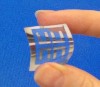
We report the fabrication and characterization of a two-terminal rewriteable nonvolatile flexible memory device that consists of a titanium dioxide layer, formed by using a room-temperature processed sol gel, with aluminum contacts on an inexpensive commercially-available flexible polymer sheet (an overhead transparency). This device shows a nonvolatile memory behavior with on/off ratios up to 1000:1, which can be cycled between write, read, and erase states by applying voltages with magnitudes of less than 10 V. The devices have the potential to meet the needs of flexible, rewritable memory while providing the advantages of simplified room temperature fabrication and relatively low drive voltage operation.

This invention allows control over the location and direction of nanowires on a large size single crystal wafer.
Pervasive devices, sensors, and networks, provide infrastructure for context-aware smart meeting rooms that sense ongoing human activities and respond to them. These technologies require advances in areas including networking, distributed computing, sensor data acquisition, signal processing, speech recognition, human identification, and natural language processing. Open interoperability and metrology standards for the sensor and recognition technologies can aid research and development programs in making these advances. To address this need the NIST Smart Space and Meeting Recognition projects are developing tools for data formats, transport, distributed processing, and metadata. We are using them to create annotated multimodal research corpora and measurement algorithms for smart meeting rooms, which we are making available to interested members of the research and development community.
We invent and demonstrate a qualitatively new form of cavity ringdown
spectroscopy utilizing a broad bandwidth optical frequency comb coherently
coupled to a high finesse optical cavity inside which molecular samples are located.
125,000 optical comb components, each coupled into a specific longitudinal cavity
mode, undergo ring down decays when the cavity input is shut off This provides
sensitive intracavity absOlption information simultaneously available across 100
nm in the visible and near IR spectral region. By placing various atomic and
molecular species (Ar, C2H2, O2, H20, NH3) inside the cavity, we demonstrate realtime,
quantitative measurements of the trace presence, transition strengths and
linewidths, and population redistributions due to collisions and temperature
changes. This novel capability to sensitively and quantitatively monitor multispecies
molecular spectra over a large optical bandwidth in real-time provides a
new spectroscopic paradigm for studying molecular vibrational dynamics, chemical
reactions, and trace analysis.
A method of simplifying a combinational circuit establishes an initial combinational circuit operable to calculate a set of target signals. A quantity of multiplication operations performed in a first portion of the initial combinational circuit is reduced to create a first, simplified combinational circuit. The first portion includes only multiplication operations and addition operations. A quantity of addition operations performed in a second portion of the first, simplified combinational circuit is reduced to create a second, simplified combinational circuit. The second portion includes only addition operations. Also, the second, simplified combinational circuit is operable to calculate the target signals using fewer operations than the initial combinational circuit.

Here we introduce a technique which allows sharp objects (e.g. scanning tunneling microscope tips, atomic force microscope tips, near-field scanning optical microscope tips, pipette tips, etc.) to be rapidly brought into close proximity to a particular region of a surface with high precision and accuracy in three dimensions. The method has potential applications in a broad array of tip-based research instrumentation and manufacturing techniques, including: scanning probe microscopy, atomic force microscopy, proximal probe lithography, dip-pen lithography, tip-indent lithography, molecule array manufacturing, and single atom manipulation.
In a typical atomic force microscope, course approach between tip and sample is achieved via a translation by a long range (0.1-1000 microns) stage followed by a fine stage movement (0.1-1000 nm); if the surface is not found, this process is repeated. Often, optical microscopes are used to aid in this process. Prior art does not allow registered tip approach due to the lack of a reliable method to yield precise three dimensional simultaneous localization of a tip and a sample surface. This knowledge is necessary in order to bring these objects into close proximity or contact with high resolution registration and speed.
Planar forms of chemically-sensitive materials have been combined, under temperature control, with the pixels of a specially-designed micro-hotplate array to produce a miniature device capable of analyzing chemical mixtures. The device uses integrated multiple elements having different adsorption properties and temperatures to collectively achieve chemical selectivity in sensing. The method of making and using selectively in sensing. The device of the present invention is manufactured by standard CMOS foundry techniques which allow the production of a range of devices that have improved sensing performance.

Disclosed is a method for operating a sensor to differentiate between first and second analytes in a sample. The method comprises the steps of determining a input profile for the sensor which will enhance the difference in the output profiles of the sensor as between the first analyte and the second analyte; determining a first analyte output profile as observed when the input profile is applied to the sensor; determining a second analyte output profile as observed when the temperature profile is applied to the sensor; introducing the sensor to the sample while applying the temperature profile to the sensor, thereby obtaining a sample output profile; and evaluating the sample output profile as against the first and second analyte output profiles to thereby determine which of the analytes is present in the sample.
Apparatus and Method Utilizing Bi-directional Relative Movement for Refreshable Tactile Display: Patent # 6,692,255
A refreshable Braille reader apparatus and method are disclosed, the apparatus preferably utilizing a rotating cylinder having endless rows of openings defined there through to a display surface with a pin held in each opening and freely movable therein. Static actuators at least equal in number to the rows of openings through the cylinder are maintained at a station adjacent to the surface of the cylinder, and are configured and positioned so that the pins are selectively contactable at either of their ends by different ones of the actuators during cylinder rotation in either forward or reverse direction thereby selectively placing first ends of the pins relative to the surface of the cylinder to allow streaming of Braille text across a display area in either forward or backward order depending upon selected direction of cylinder rotation.
A pyroelectric detector with significantly reduced microphonic noise sensitivity that includes a pyroelectric detector element constructed from a z-cut LiNbO3 or LiTaO3 electret. Selective domain reversal is accomplished in the electret by applying an electric field. Electrodes are attached to either surface of the electret spanning the domain reversed region and a portion of the original domain region to create areas of equal and opposite sensitivity. The detector is mounted in an electrically grounded container or housing. The detector may also be constructed having multiple detector regions to accommodate resonant acoustic frequencies of the electret, to function as a position sensor, or both. In other words, the position sensor has multiple domain regions that also accommodate acoustic frequencies. The detector may also be constructed having domain reversed regions placed on the electret in a periodic pattern having a geometry and spacing that is related to the acoustic impulse response of the electret. Needle domains may also be interspersed in portions or throughout the electret to scatter acoustic waves and thereby reduce acoustic noise. Multiple detectors can be produced in a simple and inexpensive manner using shadow masking techniques.